
[ad_1]
This dance, referred to as
dynamic voltage and frequency scaling (DVFS), occurs frequently within the processor, referred to as a system-on-chip (SoC), that runs your cellphone and your laptop computer in addition to within the servers that again them. It is all carried out in an effort to stability computational efficiency with energy consumption, one thing that is notably difficult for smartphones. The circuits that orchestrate DVFS try to make sure a gentle clock and a rock-solid voltage stage regardless of the surges in present, however they’re additionally among the many most backbreaking to design.
That is primarily as a result of the clock-generation and voltage-regulation circuits are analog, not like nearly every thing else in your smartphone SoC. We have grown accustomed to a near-yearly introduction of latest processors with considerably extra computational energy, because of advances in semiconductor manufacturing. “Porting” a digital design from an previous semiconductor course of to a brand new one is not any picnic, however it’s nothing in comparison with attempting to maneuver analog circuits to a brand new course of. The analog parts that allow DVFS, particularly a circuit referred to as a low-dropout voltage regulator (LDO), do not scale down like digital circuits do and should mainly be redesigned from scratch with each new technology.
If we may as an alternative construct LDOs—and maybe different analog circuits—from digital parts, they’d be a lot easier to port than some other a part of the processor, saving vital design price and releasing up engineers for different issues that cutting-edge chip design has in retailer. What’s extra, the ensuing digital LDOs might be a lot smaller than their analog counterparts and carry out higher in sure methods. Analysis teams in business and academia have examined at the very least a dozen designs over the previous few years, and regardless of some shortcomings, a commercially helpful digital LDO might quickly be in attain.
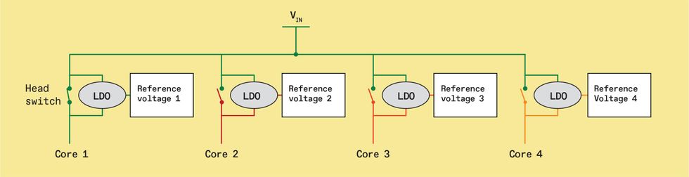
Low-dropout voltage regulators (LDOs) enable a number of processor cores on the identical enter voltage rail (VIN) to function at totally different voltages in keeping with their workloads. On this case, Core 1 has the very best efficiency requirement. Its head swap, actually a bunch of transistors linked in parallel, is closed, bypassing the LDO and immediately connecting Core 1 to VIN, which is equipped by an exterior energy administration IC. Cores 2 by 4, nevertheless, have much less demanding workloads. Their LDOs are engaged to produce the cores with voltages that may save energy.
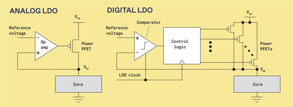
The essential analog low-dropout voltage regulator [left] controls voltage by a suggestions loop. It tries to make the output voltage (VDD) equal to the reference voltage by controlling the present by the ability PFET. Within the fundamental digital design [right], an unbiased clock triggers a comparator [triangle] that compares the reference voltage to VDD. The outcome tells management logic what number of energy PFETs to activate.
A TYPICAL SYSTEM-ON-CHIP for a smartphone is a marvel of integration. On a single sliver of silicon it integrates a number of CPU cores, a graphics processing unit, a digital sign processor, a neural processing unit, a picture sign processor, in addition to a modem and different specialised blocks of logic. Naturally, boosting the clock frequency that drives these logic blocks will increase the speed at which they get their work carried out. However to function at the next frequency, in addition they want the next voltage. With out that, transistors cannot swap on or off earlier than the following tick of the processor clock. After all, the next frequency and voltage comes at the price of energy consumption. So these cores and logic models dynamically change their clock frequencies and provide voltages—usually starting from 0.95 to 0.45 volts— based mostly on the stability of power effectivity and efficiency they should obtain for no matter workload they’re assigned—capturing video, enjoying again a music file, conveying speech throughout a name, and so forth.
Usually, an exterior power-management IC generates a number of enter voltage (VIN) values for the cellphone’s SoC. These voltages are delivered to areas of the SoC chip alongside large interconnects referred to as rails. However the variety of connections between the power-management chip and the SoC is proscribed. So, a number of cores on the SoC should share the identical VIN rail.
However they do not must all get the identical voltage, because of the low-dropout voltage regulators. LDOs together with devoted clock mills enable every core on a shared rail to function at a singular provide voltage and clock frequency. The core requiring the very best provide voltage determines the shared VIN worth. The facility-management chip units VIN to this worth and this core bypasses the LDO altogether by transistors referred to as head switches.
To maintain energy consumption to a minimal, different cores can function at a decrease provide voltage. Software program determines what this voltage must be, and analog LDOs do a reasonably good job of supplying it. They’re compact, low price to construct, and comparatively easy to combine on a chip, as they don’t require giant inductors or capacitors.
However these LDOs can function solely in a selected window of voltage. On the excessive finish, the goal voltage should be decrease than the distinction between VIN and the voltage drop throughout the LDO itself (the eponymous “dropout” voltage). For instance, if the provision voltage that might be most effective for the core is 0.85 V, however VIN is 0.95 V and the LDO’s dropout voltage is 0.15 V, that core cannot use the LDO to succeed in 0.85 V and should work on the 0.95 V as an alternative, losing some energy. Equally, if VIN has already been set under a sure voltage restrict, the LDO’s analog parts will not work correctly and the circuit cannot be engaged to cut back the core provide voltage additional.
The principle impediment that has restricted use of digital LDOs to date is the gradual transient response.
Nevertheless, if the specified voltage falls contained in the LDO’s window, software program permits the circuit and prompts a reference voltage equal to the goal provide voltage.
HOW DOES THE LDO provide the suitable voltage? Within the fundamental analog LDO design, it is via an operational amplifier, suggestions, and a specialised energy p-channel area impact transistor (PFET). The latter is a transistor that reduces its present with rising voltage to its gate. The gate voltage to this energy PFET is an analog sign coming from the op amp, starting from 0 volts to VIN. The op amp repeatedly compares the circuit’s output voltage—the core’s provide voltage, or VDD—to the goal reference voltage. If the LDO’s output voltage falls under the reference voltage—as it will when newly energetic logic all of the sudden calls for extra present—the op amp reduces the ability PFET’s gate voltage, rising present and lifting VDD towards the reference voltage worth. Conversely, if the output voltage rises above the reference voltage—as it will when a core’s logic is much less energetic—then the op amp will increase the transistor’s gate voltage to cut back present and decrease VDD.
A fundamental
digital LDO, alternatively, is made up of a voltage comparator, management logic, and numerous parallel energy PFETs. (The LDO additionally has its personal clock circuit, separate from these utilized by the processor core.) Within the digital LDO, the gate voltages to the ability PFETs are binary values as an alternative of analog, both 0 V or VIN.
With every tick of the clock, the comparator measures whether or not the output voltage is under or above the goal voltage offered by the reference supply. The comparator output guides the management logic in figuring out how lots of the energy PFETs to activate. If the LDO’s output is under goal, the management logic will activate extra energy PFETs.Their mixed present props up the core’s provide voltage, and that worth feeds again to the comparator to maintain it on the right track. If it overshoots, the comparator alerts to the management logic to change among the PFETs off.
NEITHER THE ANALOG nor the digital LDO is right, after all. The important thing benefit of an analog design is that it could reply quickly to transient droops and overshoots within the provide voltage, which is very essential when these occasions contain steep modifications. These transients happen as a result of a core’s demand for present can go up or down vastly in a matter of nanoseconds. Along with the quick response, analog LDOs are excellent at suppressing variations in VIN which may are available in from the opposite cores on the rails. And, lastly, when present calls for are usually not altering a lot, it controls the output tightly with out continually overshooting and undershooting the goal in a approach that introduces ripples in VDD.
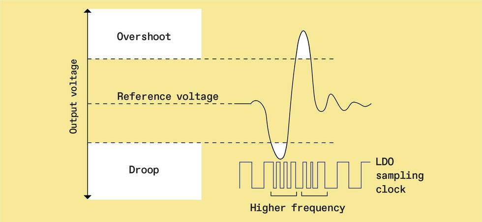
When a core’s present requirement modifications all of the sudden it could trigger the LDO’s output voltage to overshoot or droop [top]. Fundamental digital LDO designs don’t deal with this properly [bottom left]. Nevertheless, a scheme referred to as adaptive sampling with decreased dynamic stability [bottom right] can cut back the extent of the voltage tour. It does this by ramping up the LDO’s pattern frequency when the droop will get too giant, permitting the circuit to reply quicker.
Supply: S.B. Nasir et al., IEEE Worldwide Strong-State Circuits Convention (ISSCC), February 2015, pp. 98–99.
These attributes have made analog LDOs engaging not only for supplying processor cores, however for nearly any circuit demanding a quiet, regular provide voltage. Nevertheless, there are some vital challenges that restrict the effectiveness of those designs. First analog parts are rather more complicated than digital logic, requiring prolonged design occasions to implement them in superior know-how nodes. Second, they do not function correctly when VIN is low, limiting how low a VDD they’ll ship to a core. And at last, the dropout voltage of analog LDOs is not as small as designers would love.
Taking these final factors collectively, analog LDOs supply a restricted voltage window at which they’ll function. Which means there are missed alternatives to allow LDOs for energy saving—ones sufficiently big to make a noticeable distinction in a smartphone’s battery life.
Digital LDOs undo many of those weaknesses: With no complicated analog parts, they permit designers to faucet right into a wealth of instruments and different assets for digital design. So cutting down the circuit for a brand new course of know-how will want a lot much less effort. Digital LDOs may also function over a wider voltage vary. On the low-voltage finish, the digital parts can function at VIN values which can be off-limits to analog parts. And within the increased vary, the digital LDO’s dropout voltage will probably be smaller, leading to significant core-power financial savings.
However nothing’s free, and the digital LDO has some critical drawbacks. Most of those come up as a result of the circuit measures and alters its output solely at discrete occasions, as an alternative of repeatedly. Which means the circuit has a relatively gradual response to produce voltage droops and overshoots. It is also extra delicate to variations in VIN, and it tends to provide small ripples within the output voltage, each of which may degrade a core’s efficiency.
Of those, the primary impediment that has restricted the usage of digital LDOs to date is their gradual transient response. Cores expertise droops and overshoots when the present they draw abruptly modifications in response to a change in its workload. The LDO response time to droop occasions is vital to limiting how far voltage falls and the way lengthy that situation lasts. Typical cores add a security margin to the provision voltage to make sure right operation throughout droops. A larger anticipated droop means the margin should be bigger, degrading the LDO’s energy-efficiency advantages. So, dashing up the digital LDO’s response to droops and overshoots is the first focus of the cutting-edge analysis on this area.
SOME RECENT ADVANCES have helped velocity the circuit’s response to droops and overshoots. One method makes use of the digital LDO’s clock frequency as a management knob to commerce stability and energy effectivity for response time.
A decrease frequency improves LDO stability, just because the output won’t be altering as usually. It additionally lowers the LDO’s energy consumption, as a result of the transistors that make up the LDO are switching much less regularly. However this comes at the price of a slower response to transient present calls for from the processor core. You possibly can see why that might be, in case you contemplate that a lot of a transient occasion may happen inside a single clock cycle if the frequency is simply too low.
Conversely, a excessive LDO clock frequency reduces the transient response time, as a result of the comparator is sampling the output usually sufficient to alter the LDO’s output present earlier within the transient occasion. Nevertheless, this fixed sampling degrades the steadiness of the output and consumes extra energy.
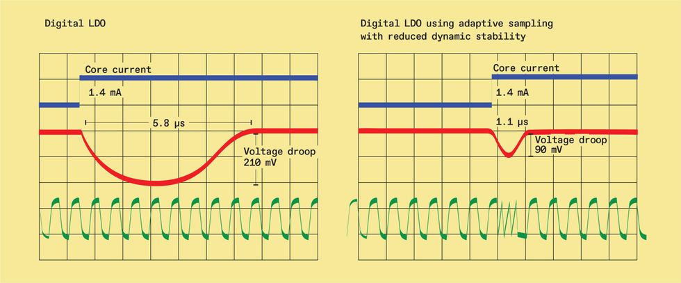
The gist of this method is to introduce a clock whose frequency adapts to the scenario, a scheme referred to as adaptive sampling frequency with decreased dynamic stability. When voltage droops or overshoots exceed a sure stage, the clock frequency will increase to extra quickly cut back the transient impact. It then slows all the way down to devour much less energy and preserve the output voltage steady. This trick is achieved by including a pair of further comparators to sense the overshoot and droop circumstances and set off the clock. In measurements from a check chip utilizing this system, the VDD droop decreased from 210 to 90 millivolts—a 57 p.c discount versus a normal digital LDO design. And the time it took for voltage to settle to a gentle state shrank to 1.1 microseconds from 5.8 µs, an 81 p.c enchancment.
Another method for enhancing the transient response time is to make the digital LDO somewhat bit analog. The design integrates a separate analog-assisted loop that responds immediately to load present transients. The analog-assisted loop {couples} the LDO’s output voltage to the LDO’s parallel PFETs by a capacitor, making a suggestions loop that engages solely when there’s a steep change in output voltage. So, when the output voltage droops, it reduces the voltage on the activated PFET gates and instantaneously will increase present to the core to cut back the magnitude of the droop. Such an analog-assisted loop has been proven to cut back the droop from 300 to 106 mV, a 65 p.c enchancment, and overshoot from 80 to 70 mV (13 p.c).
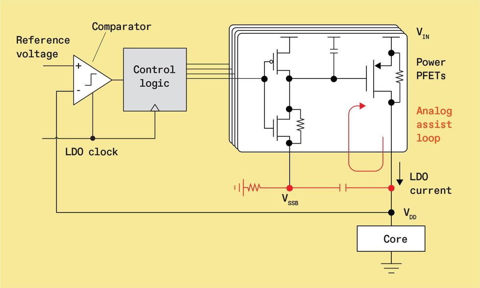

Another option to make digital LDOs reply extra shortly to voltage droops is so as to add an analog suggestions loop to the ability PFET a part of the circuit [top]. When output voltage droops or overshoots, the analog loop engages to prop it up [bottom], lowering the extent of the tour.
Supply: M. Huang et al., IEEE Journal of Strong-State Circuits, January 2018, pp. 20–34.
After all, each of those strategies have their drawbacks. For one, neither can actually match the response time of right this moment’s analog LDOs. As well as, the adaptive sampling frequency method requires two further comparators and the technology and calibration of reference voltages for droop and overshoot, so the circuit is aware of when to have interaction the upper frequency. The analog-assisted loop consists of some analog parts, lowering the design-time good thing about an all-digital system.
Developments in business SoC processors might assist make digital LDOs extra profitable, even when they cannot fairly match analog efficiency. In the present day, business SoC processors combine all-digital adaptive circuits designed to mitigate efficiency issues when droops happen. These circuits, for instance, briefly stretch the core’s clock interval to forestall timing errors. Such mitigation strategies may loosen up the transient response-time limits, permitting the usage of digital LDOs and boosting processor effectivity. If that occurs, we will count on extra environment friendly smartphones and different computer systems, whereas making the method of designing them a complete lot simpler.
[ad_2]